Contact: Guillaume Agnus
PhD students : Hidayat Elourajini
Postdoc : Pierre Taugeron
Former PhD students : Ngoc Thi Nguyen, David le Bourdais, Sopheasith Hem, Subhajit Roy
Context:
Functional perovskite oxides are of great interest for fundamental and applied research thanks to the numerous physical properties and inherent mechanisms they display. With the maturation of thin film deposition techniques, research teams are able to produce oxide films and nanostructures of great crystalline quality with some of the most remarkable properties found in physics, a state leading now to upper-level thoughts like their ability to fulfill industrial needs.
OXIDE team aims at answering to some of the problematics that arise when considering the oxide transition from the research to the industrial world, focusing on their integration for micro-electro-mechanical devices (MEMS) such as sensors.
Project:
Perovskites exhibit several advantages in order to use them as active material for sensors. First, their exceptional physical properties allow to enhance the sensitivity of the sensors, combined in some cases with a drastic reduction of the power consumption. Then, the very high stability of this class of materials, in particular with respect to oxygen, allows to use the sensors in very harsh environment. Finally, it is possible to take advantage not only of the properties of one material but to couple the properties of several of them thanks to heteroepitaxial growth of perovskite stacks.
Since more than 15 years, we have developed the growth by Pulsed Laser Deposition of complex heterostructures first on conventional perovskite substrates but also on Silicon substrate, that open up for the realization of MEMS based on perovskites.
We have developed two major research activities on that topic:
This multi-disciplinary project covers a broad range of research fields as follows:
|
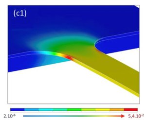
Finite Element Modelling (FEM) in order to design the best possible device geometry
|
FEM simulation of the stress in manganite freestanding bridge (Le Bourdais PhD) |
|
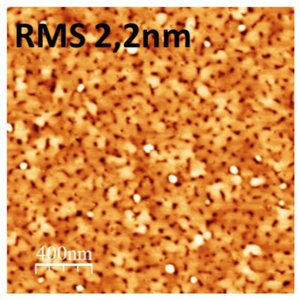
AFM image of a PZT thin film on YSZ-buffered Silicon (Nguyen PhD) |
Thin films growth: Perovskite thin films are epitaxially grown by Pulsed-Laser Deposition (PLD) and their structural quality is studied by X-ray diffraction (XRD) and Atomic Force Microscopy (AFM). Equipments: PLD, XRD, AFM.
|
|
Patterning the devices: The structures are patterned down to the micro-nanometer scale, using several clean room processes, to define the required geometries. Equipments: Optical lithography, e-Beam lithography, sputtering, evaporation, etching (RIE, IBE) in clean room.
|
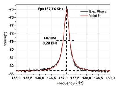
SEM images of freestanding manganite cantilevers |
|
Resonant frequency of a freestanding magnetostrictive cantilever (Nguyen PhD) |
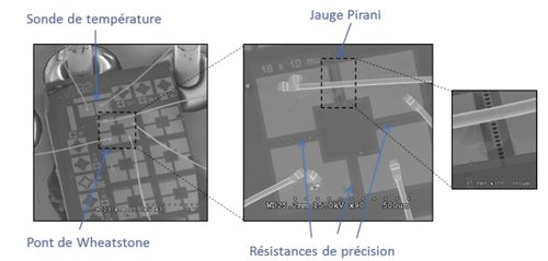
Electrical characterizations: Many techniques are used such as current vs voltage (I-V), capacitance vs voltage (C-V), resistance vs pressure (R-P) or temperature (R-T), and resonant frequency measurements. Equipments: Sourcemeters, Impedance-meters, ferroelectric tester and home made measurement tools.
|